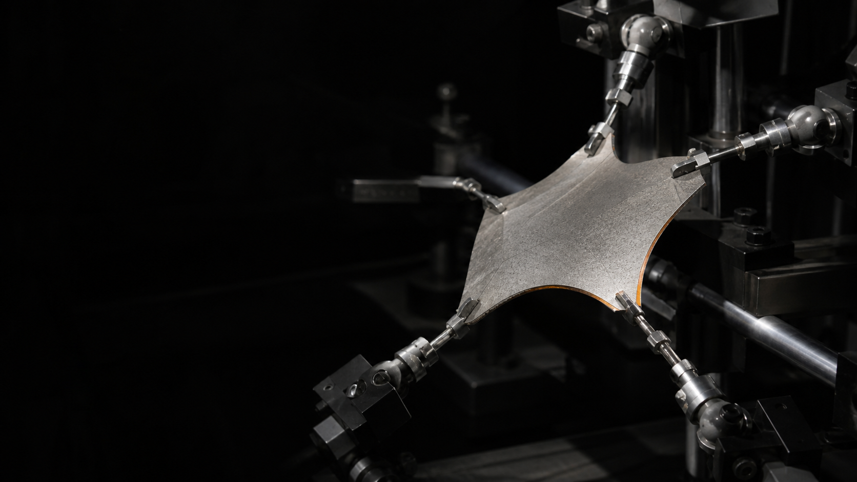
Standard semiconductor manufacturing can now produce freestanding, stable three-dimensional objects with curved surfaces directly from flat wafers. Semiconductor fabrication historically created only flat chips or bendable planar sheets rather than rigid curved structures. The new method mathematically flattens a curved target design into a flat mesh of microscopic unit cells that pop into a second stable shape when pressed.
Each unit cell in the flat pattern is tuned so that outward expansion triggers a second resting equilibrium. When an external force pushes the material, the connected cells snap outward together like an umbrella popping open. This collective mechanical jump locks the entire flat sheet into a preplanned three-dimensional curvature. The design method works across both positive curves like domes and negative saddle shapes.
The research team tested the generative technique by fabricating a flat circular disk designed to become a spherical dome under mechanical indentation. Numerical simulations and laboratory measurements confirmed that the disk snapped accurately into the target geometry while remaining structurally stable. The engineers also built curved paraboloidal reflectors whose measured light reflections matched predictions from geometric optics.
According to the authors, this manufacturing technique bridges flexible electronics and deployable three-dimensional electronics. The method broadens the range of realizable semiconductor devices to include curved reflectors and antennas with tunable focal lengths.